AVS hosted a double feature:
Prof. Krogstad (Asst. Professor, Department of Materials Science and Engineering) discussed how a fundamental understanding of local microstructural evolution, thermodynamic and kinetic driving forces, and mechanical response can be used to improve the long-term response of materials under extreme conditions.
Prof. Huang (Asst. Professor, Department of Materials Science and Engineering) then discussed her TEM investigations into 2-d material interfaces with single-atom precision. She focused on methods for investigating the atomic structure around these interfaces and tied these defects to electronic structure and properties.
Tuesday, December 1, 2015

Monday, August 17, 2015
Joint AVS-MRS Argonne National Laboratory Trip

Thursday, June 4, 2015
AVS and Asylum Research, an Oxford Instruments Company seminar on Scanning Microwave Impedance Microscopy and XRD characterization of ion-damaged single crystals
Double Feature:
 Dr. Ted Limpoco of Asylum Research, an Oxford Instruments Company discussed the basics of SMIM, an atomic force microscopy-based technique, and the types of information that can be attained using the technique. This technique can be used to probe the impedance of the tip-sample interface and learn about the local electrical properties.
 Dr. Kirill D. Shcherbachev of the Russian National University of Science and Technology discussed advanced HR-XRD techniques for characterizing ion-damaged single crystals. The techniques discussed may be used to attain a damage depth distribution using the shape of the diffraction curve, separating coherently and incoherently scattered x-rays.
 Dr. Ted Limpoco of Asylum Research, an Oxford Instruments Company discussed the basics of SMIM, an atomic force microscopy-based technique, and the types of information that can be attained using the technique. This technique can be used to probe the impedance of the tip-sample interface and learn about the local electrical properties.
Friday, March 13, 2015
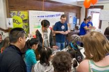
Engineering Open House 2015
 Unfortunately, the camera broke, so here is a picture from a prior year, but we did more vacuum demonstrations for kids at the 2015 Engineering Open House on Mar. 13. Thank you to all who were able to help out!
Friday, November 21, 2014
Outreach to 5th Grade Students with St. Elmo Brady STEM academy

On Oct. 25, the University of Illinois AVS Student Chapter taught ~ 15 4th and 5th grade boys of the St. Elmo Brady STEM academy about vacuum science. The St. Elmo Brady STEM academy gives African-American 4th and 5th grade boys hands-on exposure to science, technology, engineering and mathematics. We showed them what happens to a ringing alarm clock, the speed at which a feather and magnet fall, Peeps, shaving cream, a candle, a balloon, and water in a vacuum and helped them to discover why these materials behave the way that they do in a vacuum.
Wednesday, September 17, 2014
Tatyana Kuznetsova and Vladimir Grebennikov of the Russian Academy of Sciences Seminar
On Wednesday, Sept. 17, Drs. Kuznetsova and Grebennikov discussed their investigations into topological insulators using angle-resolved photoelectron spectroscpoy (ARPES) and scanning tunneling microscopy/spectroscopy (STM/STS).
Bismuth tellurohalides including BiTeI belong to a family of layered polar semiconductors lacking inversion symmetry. Much attention has recently been paid to these compounds due to the strong spin-orbit interactions of electrons caused by Bi atoms. The strong correlation between the direction of motion and spin of charge carriers (called the Rashba splitting) in materials without spatial inversion can be used in spintronic devices. The Rashba effect leads to a shift of opposite spin-polarized bands in opposite directions on the momentum scale. In the semiconductor BiTeI, the Rashba effect can be used to control the spin of charge carriers using electric fields providing a pathway for the technological development of spintronic devices.
The near surface layer of BiTeI has been converted to the three-dimensional topological insulator state by doping the surface with Cs. We studied this system by angle-resolved photoelectron spectroscopy (ARPES) and scanning tunneling spectroscopy. We analyzed the electronic structure of the (0001) surface of BiTeI and its modification upon adsorption of Cs using ARPES. A strong shift of the electronic states at the (0001) BiTeI surface by several hundred meV to higher binding energies due to band bending effects as well as the Rashba splitting are observed. Both scanning tunneling microscopy (STM) and spectroscopy (STS) show unusual atomic structures of the surfaces terminated by both tellurium and iodine atoms. Our experiments have shown that the relaxation of the surface atoms in these compounds is significant and can be used to control surface states in topological insulators.
Bismuth tellurohalides including BiTeI belong to a family of layered polar semiconductors lacking inversion symmetry. Much attention has recently been paid to these compounds due to the strong spin-orbit interactions of electrons caused by Bi atoms. The strong correlation between the direction of motion and spin of charge carriers (called the Rashba splitting) in materials without spatial inversion can be used in spintronic devices. The Rashba effect leads to a shift of opposite spin-polarized bands in opposite directions on the momentum scale. In the semiconductor BiTeI, the Rashba effect can be used to control the spin of charge carriers using electric fields providing a pathway for the technological development of spintronic devices.
The near surface layer of BiTeI has been converted to the three-dimensional topological insulator state by doping the surface with Cs. We studied this system by angle-resolved photoelectron spectroscopy (ARPES) and scanning tunneling spectroscopy. We analyzed the electronic structure of the (0001) surface of BiTeI and its modification upon adsorption of Cs using ARPES. A strong shift of the electronic states at the (0001) BiTeI surface by several hundred meV to higher binding energies due to band bending effects as well as the Rashba splitting are observed. Both scanning tunneling microscopy (STM) and spectroscopy (STS) show unusual atomic structures of the surfaces terminated by both tellurium and iodine atoms. Our experiments have shown that the relaxation of the surface atoms in these compounds is significant and can be used to control surface states in topological insulators.
Tuesday, September 16, 2014
Michael V. Yakushev, University of Strathclyde UK Seminar
On Tues. Sept 16, Dr. Yakushev was able to teach us about the capabilities of optical spectroscopy including photoluminescence by describing his work with chalcopyrites and other semiconductors.
The chalcopyrite semiconductors based on CuInSe2 are key components in the absorber layer of solar cells which are amongst leading thin-film PV technologies in terms of efficiency and stability. These solar cells have been developed mostly using empirical approaches rather than scientific knowledge-based design: it worked first and was explained later. As a result the progress of the chalcopyrite-based solar cells shows a clear saturation towards not 30 %, a theoretical limit for single-junction solar cells, but 21 %. The problem seems to be that the materials are too complicated for an empirical design.
A solution could be in studying first high structural quality model materials and then using the obtained knowledge for technology grade materials. That is how all other successful semiconductor technologies have been developed. A signficant improvement in the quality of the chalcopyrites produced in Strathclyde facilitated the use of fine methods of optical and magneto-optical spectroscopy to study excitonic states and helped to determine a number of fundamental electronic properties.
The next step in the development of the chalcopyrites is the substitution of rare and expensive In and Ga with alternating Zn and Sn: Cu2ZnSn(SeS)4 with a kesterite structure. An encouraging efficiency in excess of 11 % has already been reported for solar cells based on this compound. However, the material might be far too complicated whereas some other compounds like Cu3BiS3 can probably offer a simpler solution.
Friday, April 25, 2014
Christian Schlepuetz Seminar

The past couple of years have marked the centennial anniversary of x-ray crystallography - a field of research that has seen a tremendous growth ever since its birth. Rather than going out of fashion eventually, it has helped to push the boundaries of our understanding of matter and materials steadily further. New x-ray techniques are continuously added to our set of available research tools, while established methods of crystallograpy are reaching new frontiers by taking advantage of the latest instrumentation developments.
 The exploration of reciprocal space has taken a leap in terms of speed, accuracy, reliability, and the obtainable level of detail with the advent of modern single-photon-counting x-ray area detectors featuring high frame rates and zero readout noise. Each detector image represents a 2-dimensional slice through reciprocal space, and a single diffractometer scan extends this to a stack of slices probing a 3-dimensional volume. This allows for the rapid characterization of large volumes of reciprocal space, revealing all of the structural phases and their orientations present in a sample. The method is particularly powerful if not all the constituent phases and the corresponding locations of their diffraction signals are known, and aids in the discovery of unexpected phenomena or crystal structures.
In this talk, Christian gave a basic tutorial on how to navigate in reciprocal space and showed how to use a Pilatus 100K pixel detector to collect large volume data sets, which could then be processed to yield 3-dimensional reciprocal space maps (RSMs), high-quality powder diffraction data, or simultaneous measurements of pole figures for a whole range of 2-theta values. The capabilities of this approach were then highlighted using several topical research examples: The detailed investigation of the domain structure of multiferroic bismuth ferrite (BiFeO3) thin films and its phase transitions with temperature and film thickness was only possible due to the rapid collection of many RSMs, including those around the half-order film Bragg Peaks, which contain sensitive information about the oxygen octahedra rotation patterns in this material. Iron oxide (Fe2O3), as another example, is an attractive material for the photoelectrochemical (PEC) oxidation of water, particularly when it is heteroepitaxially grown on the facets of indium tin oxide (ITO) nanowires to form a core-shell structure with a large catalytic surface area, long optical absoption paths, and short charge transfer pathways. Simultaneous pole figure measurements of the ITO and Fe2O3 diffraction signals help to reveal the epitaxial relationship at the interface between the ITO nanowire facets and the Fe2O3 layer and provide information which can ultimately be used to guide the design and optimization of future PEC devices.
Saturday, March 15, 2014
Engineering Open House 2014

Vacuums are more than your trusty Hoover! They are used in a wide variety of industries and can be used to illustrate many important physical concepts, such as pressure, phase changes, and acoustics. Have you ever wondered what would happen to a balloon in a vacuum? Could you hear an explosion in space? What happens to fire in the vacuum of space? Can you get a fireball in space? How can you get ice to crystallize at room temperature? What happens when you put Peeps and shaving cream in a vacuum?
Thank you to all who helped to man the booth!


Friday, November 8, 2013
Jasprit Singh Seminar

Professor Jasprit Singh from the Department of Electrical Engineering and Computer Science at the University of Michigan, Ann-Arbor, discussed how technology can be used to bring harmony to our lives. In today’s age of “knowledge abundance” a key challenge is to bring harmony between knowledge and action. Our modern age may be called the age of mindfulness where lack of mindfulness is reflected in the gap between resources, knowledge and action. Human consumption has never been higher but more than a third of human actions worldwide are taken to undo our previous actions. This represents the “Carnot efficiency” of modern life. The obesity crisis, the environmental crisis as well as global economic crisis are not primarily due to a lack of knowledge or resources but due to our inability to act on what we know and want.
What role can technology play to harmonize what we know, what we want and what we do? What kinds of sensors and devices are needed for making this happen? In this talk I will describe some of the potential roles technology can play in acting as a “mentor” in our life. In particular I will describe our work on mobile “mentor platforms” and describe the potential role of new materials and sensors that could be integrated in mobile or wearable devices.
Friday, September 20, 2013
Peter Voorhees Seminar

Professor Voorhees of Northwestern University’s Department of Materials Science came to the University of Illinois Champaign-Urbana to discuss his research into vapor-liquid-solid nanowire growth. Faculty and students, alike learned new techniques and analysis methods. His group used video-rate lattice-resolved environmental transmission electron microscopy to show in-situ the nanowire growth interface during growth. He found that, due to the nanowire geometry, a single twin boundary is located at the nanowire center. This twin acts as a preferential nucleation site from which the nanowire grows. He also discussed a model that he used to demonstrate the manner in which the catalyst droplet becomes unstable and compared the predictions of this simulation to experimental observations.
Monday, December 10, 2012
Mark Hersam Seminar


Thursday, October 25, 2012
Fermilab 2012
The operation of the Tevatron, the world’s second largest particle accelerator, at Fermilab was a coalition of efforts by numerous physics, material scientists, and engineers from diverse backgrounds ranging from particle physics, to polymer science and superconductivity. In our trip to the accelerator, measuring 1 kilometer in diameter, the AVS group had a chance visit many of the sites along its perimeter, while talking the primary actors involved in continuing the legacy left by the discovery of the bottom Omega baryon. Amongst the various sites seen, the group had an opportunity to tour within the DZero detector!

Friday, April 20, 2012
James Coleman Seminar
 Semiconductor quantum dot lasers have been extensively studied for applications in future lightwave telecommunications systems. Prof. Coleman described the growth, processing and characteristics of quantum dot and nanostructure lasers that exhibit interesting and potentially important effects arising from reduction of the active medium to the quantum regime (<50 nm) in all three dimensions. The motivation for quantum dots in lasers was outlined along with methods for forming self-assembled and patterned quantum dots. The resultant laser characteristics was presented. Prof. Coleman introduced a novel inverted quantum dot structure or nanopore laser, containing three dimensional quantization formed from an engineered periodicity.

Wednesday, April 18, 2012
Vacuum Workshop 2012

Two-day vacuum workshop on April 17th and 18th 2012 from 11:00-1:00 pm in MRL 280!
Do you work with vacuum systems?
PLD? MBE? CVD? ALD? Sputtering?
Ever wonder how to build a vacuum chamber?
Ever wonder why your base pressure is too high?
Ever wonder what materials are vacuum compatible?
Ever wonder how to use a leak detector?
These are some of the questions we will be addressing at our two day vacuum workshop on April 17th and 18th from 11:00-1:00 pm in MRL 280!
The full list of topics are: gas and surface physics, vacuum technology, industry standards, component design and fabrication, system operation and safety.
Lunch will be provided.
To attend pre-register with the form at the bottom of this page. (Registration is now closed.)
Hosted by UIUC AVS Student Chapter. Presented by A&N Coorporation (http://www.ancorp.com/).
For more information, contact Frank Bergschneider at Fberg@ancorp.com or the UIUC AVS Student Chapter at illinoisavs@gmail.com
Friday, March 9, 2012
Engineering Open House 2012

At Engineering Open House, the AVS Student Chapter held exhibitions to introduce kids and adults to the fun of vacuum science. One exhibition involved the effects of atmospheric pressure on everyday objects, or more specifically: what would happen to peeps and shaving cream in space! Another bewildered even adults by freezing water after making it boil in a vacuum! Be sure to see our videos: peep in a vacuum, shaving cream in a vacuum, boiling water that freezes in a vacuum, balloon in vacuum, and candle in a vacuum!


Saturday, February 11, 2012
Anthony Leggett Seminar


Friday, October 28, 2011
Milan Mirksich Seminar

The necessity to identify the plethora of still unknown biomarkers and reaction pathways required to individualize therapeutics to patient-specific phenotypes or to mass distribute cost effective microfluidic assaying devices to developing counties is pressing. However, the daunting number of unique compounds and reactions playing important roles renders any attempt at progress without high throughput considerations ludicrous.
Prof. Mirksich described an approach for using mass spectrometry to analyze self-assembled monolayers of alkanethiolates on gold. This technique, termed SAMDI MS, can efficiently identify the masses of substituted alkanethiolates in the monolayer and therefore enables the use of monolayers to assay a broad class of enzyme activities — including kinase, protease, methyltransferase and carbohydrate-directed modifications — and for discovering chemical reactions. In the seminar, he described applications for high throughput experiments, including the construction of peptide arrays and their use to profile the deacetylase and acetyl transferase family of enzymes, and to explore non-intuitive ways in which networks of enzymes can control protein acetylation.
Friday, October 7, 2011
Dmitri Talapin Seminar

The necessity to identify the plethora of still unknown biomarkers and reaction pathways required to individualize therapeutics to patient-specific phenotypes or to mass distribute cost effective microfluidic assaying devices to developing counties is pressing. However, the daunting number of unique compounds and reactions playing important roles renders any attempt at progress without high throughput considerations ludicrous.
Prof. Mirksich described an approach for using mass spectrometry to analyze self-assembled monolayers of alkanethiolates on gold. This technique, termed SAMDI MS, can efficiently identify the masses of substituted alkanethiolates in the monolayer and therefore enables the use of monolayers to assay a broad class of enzyme activities — including kinase, protease, methyltransferase and carbohydrate-directed modifications — and for discovering chemical reactions. In the seminar, he described applications for high throughput experiments, including the construction of peptide arrays and their use to profile the deacetylase and acetyl transferase family of enzymes, and to explore non-intuitive ways in which networks of enzymes can control protein acetylation.
Monday, October 25, 2010
Fermilab 2010
The operation of the Tevatron, the world’s second largest particle accelerator, at Fermilab was a coalition of efforts by numerous physics, material scientists, and engineers from diverse backgrounds ranging from particle physics, to polymer science and superconductivity. In our trip to the accelerator, measuring 1 kilometer in diameter, the AVS group had a chance visit many of the sites along its perimeter, while talking the primary actors involved in continuing the legacy left by the discovery of the bottom Omega baryon.

Subscribe to:
Posts (Atom)